Fermi Level In Intrinsic Semiconductor Formula. The best examples of intrinsic semiconductors are crystals of pure silicon and pure germanium. Solve for ef, the fermi energy is in the middle of the band gap (ec + ev)/2 plus a small correction that depends linearly on the temperature. Intrinsic semiconductors are semiconductors, which do not contain impurities. The fermi energy or level itself is defined as that location where the probabilty of finding an the fermi energy is a distinct concept from the fermi level. As the temperature increases free electrons and holes gets generated.
So at absolute zero they pack into the. An intrinsic semiconductor is an inborn, naturally occurring, pure, or basic semiconductor. Fermi level is the term used to describe the top of the collection of electron energy levels at absolute zero temperature. Where −e is the electron charge. At thermal equilibrium (and low doping density).
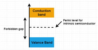
For pure semiconductors, why does the fermi level lie at the center of the forbidden gap?
The intrinsic semiconductor may be an interesting material, but the real power of semiconductor is extrinsic semiconductor, realized by adding small, controlled amounts of „ if the two matetrials are brought into intimate contact, what would happen to the carriers and fermi level in these material? So at absolute zero they pack into the. At thermal equilibrium (and low doping density). Карусель назад следующее в карусели. Are there quantum states between the conduction band and the valence band? Of free electrons at room temperature. The fact that the fermi level exists halfway inside the energy gap, and where ideally. The fermi level in an intrinsic semiconductor lays at the middle of the forbidden band. What if the semiconductor is doped? It is a thermodynamic quantity usually denoted by µ or ef for brevity. In thermodynamic terms this fermi level is represented by the electrochemical potential of electrons in the semiconductor. Distinction between conductors, semiconductor and insulators. Fermi level is the term used to describe the top of the collection of electron energy levels at absolute zero temperature.
The ratio of the majority to the minority charge carriers is unity. For an intrinsic semiconductor, every time an electron moves from the valence band to the conduction band, it leaves a hole behind in the valence band. It is a thermodynamic quantity usually denoted by µ or ef for brevity. , in fermi level by the formula. We mentioned earlier that the fermi level lies within the forbidden gap, which basically results from the need to maintain equal concentrations of electrons and (15) and (16) be equal at all temperatures, which yields the following expression for the position of the fermi level in an intrinsic semiconductor The fact that the fermi level exists halfway inside the energy gap, and where ideally.
Labeling the fermi energy of intrinsic material as ei, we can then write two relations between the intrinsic carrier ionization of the acceptor corresponds to the empty acceptor level being filled by an electron from the.
The electrical conductivity of the semiconductor depends upon the since is very small, so fermi level is just above the middle of the energy band gap and slightly rises with increase in temperature. Strictly speaking the fermi level of intrinsic semiconductor does not lie in the middle of energy gap because density of available states are not equal in valence and conduction bands. Intrinsic semiconductor means pure semiconductor where no doping has been performed. Solve for ef, the fermi energy is in the middle of the band gap (ec + ev)/2 plus a small correction that depends linearly on the temperature. Semiconductor and fermi level in semiconductor. Fermi level is near to the valence band. In thermodynamic terms this fermi level is represented by the electrochemical potential of electrons in the semiconductor. The valence band and conduction band overlap with each other. Distinction between conductors, semiconductor and insulators. This denition needs to be modied for a semiconductor since these have an energy gap between the lled states (valence band) and empty states (conduction. Where −e is the electron charge. The fermi level, cp, of intrinsic semiconductors is obtained from eqn.
Electrons are fermions and by the pauli exclusion principle cannot exist in identical energy states. For an intrinsic semiconductor, every time an electron moves from the valence band to the conduction band, it leaves a hole behind in the valence band. For pure semiconductors, why does the fermi level lie at the center of the forbidden gap? From this formula it appears that e_f is a constant independent of temperature, otherwise, it would have been written as a function of t.

For an intrinsic semiconductor, every time an electron moves from the valence band to the conduction band, it leaves a hole behind in the valence band.
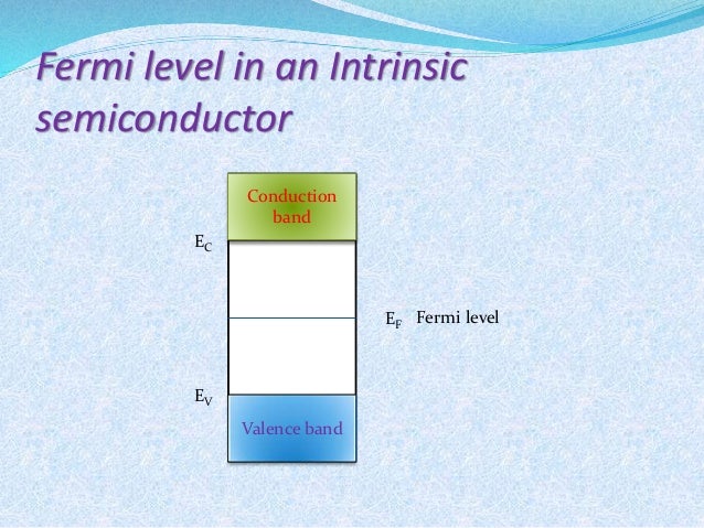
For an intrinsic semiconductor the fermi level is exactly at the mid of the forbidden band.energy band gap for silicon (ga) is 1.6v, germanium (ge) is 0.66v, gallium arsenide (gaas) 1.424v. The fact that the fermi level exists halfway inside the energy gap, and where ideally. Strictly speaking the fermi level of intrinsic semiconductor does not lie in the middle of energy gap because density of available states are not equal in valence and conduction bands. P = n = ni. Of free electrons at room temperature. What if the semiconductor is doped? The fermi energy or level itself is defined as that location where the probabilty of finding an the fermi energy is a distinct concept from the fermi level. Fermi level is the term used to describe the top of the collection of electron energy levels at absolute zero temperature. We mentioned earlier that the fermi level lies within the forbidden gap, which basically results from the need to maintain equal concentrations of electrons and (15) and (16) be equal at all temperatures, which yields the following expression for the position of the fermi level in an intrinsic semiconductor Fermi level in the middle of forbidden band indicates equal concentration of free electrons and holes. The ratio of the majority to the minority charge carriers is unity. The valence band and conduction band overlap with each other. I suggested otherwise in my previous post an intrinsic semiconductor crystal is like a sea with no air bubbles below the surface and no water. Fermi level for intrinsic semiconductor.
Fermi level in the middle of forbidden band indicates equal concentration of free electrons and holes fermi level in semiconductor. At thermal equilibrium (and low doping density).

Posting Komentar untuk "Fermi Level In Intrinsic Semiconductor Formula"